Product Applications
GEPON OLT For P2MP Application
General
The HDV ZL5432099-ICS transceiver with supports data rate of typical 1.25 Gbps for GEPON OLT application up to 20km transmission distance, it’s designed meeting with China Telecom EPON equipment technical requirement V2.1 1000BASE-PX20+ specifications. SC rececptacle is for optical interface.
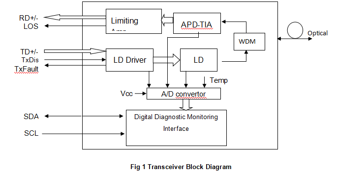
The module provides digital diagnostic information of its operating conditions and status, including transmitting power, laser bias, receiver input optical power, module temperature, and supply voltage. Calibration and alarm/warning threshold data are written and stored in internal memory (EEPROM). The memory map is compatible with SFF-8472, as shown in Fig. 2. The diagnostic data are raw A/D values and must be converted to real world units using calibration constants stored in EEPROM locations 56 – 95 in A2h.
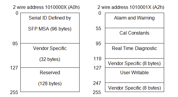
Fig 2 EEPROM Information
Performance Specifications
|
Absolute Maximum Ratings |
|||||||||||
|
Parameter |
Symbol |
Min. |
Max. |
Unit |
Note |
||||||
|
Storage Temperature
|
Tst |
-40 |
+85 |
°C |
|||||||
|
Operating Case Temperature |
Tc |
0 |
70 |
°C |
|||||||
|
Input Voltage |
- |
GND |
Vcc |
V |
|||||||
|
Power Supply Voltage |
Vcc-Vee |
-0.5 |
+3.6 |
V |
|||||||
| Recommended Operating Conditions | |||||||||||
|
Parameter |
Symbol |
Min. |
Typical |
Max. |
Unit |
Note | |||||
|
Power Supply Voltage |
Vcc |
3.135 |
3.3 |
3.465 |
V |
||||||
|
Operating Case Temperature |
Tc |
0 |
- |
70 |
°C |
||||||
|
Data Rate |
DR |
- |
1.25 |
- |
Gbps |
||||||
|
Total Supply Current |
- |
- |
- |
400 |
mA |
||||||
|
Damage Threshold For Receiver |
- |
- |
- |
4 |
dBm |
||||||
|
Optical Specification |
||||||
|
Transmitter |
||||||
|
Parameter |
Symbol |
Min. |
Typ. |
Max. |
Unit |
Note |
| Optical Central Wavelength |
l |
1480 |
1490 |
1500 |
nm |
- |
|
Spectral Width (-20dB) |
Dl |
- |
- |
1 |
nm |
- |
|
Side Mode Suppression Ratio |
SMSR |
30 |
- |
- |
dB |
- |
|
Average Optical Output Power |
Po |
+3 |
- |
+7 |
dBm |
- |
|
Extinction Ratio |
Er |
9 |
- |
- |
dB |
- |
|
Rise/Fall Time |
Tr/Tf |
- |
- |
260 |
ps |
- |
|
Transmitter Total Jitter |
Jp-p |
- |
- |
344 |
ps |
|
|
Transmitter Reflectance |
RFL |
- |
- |
-12 |
dB |
|
|
Average Lauched Power of Off Transmitter |
Poff |
- |
- |
-39 |
dBm |
- |
|
Differential Input Voltage |
VIN-DIF |
300 |
- |
1600 |
mV |
- |
|
Tx Disable Input Voltage-Low |
VIL |
0 |
- |
0.8 |
V |
- |
|
Tx Disable Input Voltage-High |
VIH |
2.0 |
- |
Vcc |
V |
- |
|
Output Eye |
Compliant with IEEE 802.3ah-2004 |
|||||
|
Receiver |
||||||
|
Parameter |
Symbol |
Min. |
Typ. |
Max. |
Unit |
Note |
|
Operate Wavelength |
- |
1280 |
1310 |
1340 |
nm |
- |
|
Sensitivity |
Pr |
- |
- |
-30 |
dBm |
1 |
|
Saturation |
Ps |
-6 |
- |
- |
dBm |
1 |
|
LOS assert Level |
- |
-45 |
- |
- |
dBm |
- |
|
LOS De-Assert Level |
- |
- |
- |
-30 |
dBm |
- |
|
LOS Hysteresis |
- |
0.5 |
- |
5 |
dB |
- |
|
Receiver Optical Reflectance |
- |
- |
- |
-12 |
dB |
- |
|
Data Output Low |
Vol |
-2 |
- |
-1.58 |
V |
- |
|
Data Output High |
Voh |
-1.1 |
- |
-0.74 |
V |
- |
|
LOSOutput Voltage-Low |
VSD-L |
0 |
- |
0.8 |
V |
- |
|
LOS Output Voltage-High |
VSD-H |
2.0 |
- |
Vcc |
V |
|
Note:
1. Minimum Sensitivity and saturation levels for an 8B10B 27-1 PRBS. BER≤10-12, 1.25Gpbs, ER=9dB
EEPROM Information
EEPROM Serial ID Memory Contents (A0h)
|
Addr. (decimal) |
Field Size (Bytes) |
Name of Field |
Content (Hex) |
Content (Decimal) |
Description |
|
0 |
1 |
Identifier |
03 |
3 |
SFP |
|
1 |
1 |
Ext. Identifier |
04 |
4 |
MOD4 |
|
2 |
1 |
Connector |
01 |
1 |
SC |
|
3-10 |
8 |
Transceiver |
00 00 00 80 00 00 00 00 |
00 00 00 128 00 00 00 00 |
EPON |
|
11 |
1 |
Encoding |
01 |
1 |
8B10B |
|
12 |
1 |
BR, nominal |
0C |
12 |
1.25Gbps |
|
13 |
1 |
Reserved |
00 |
0 |
- |
|
14 |
1 |
Length (9um)-km |
14 |
20 |
20/km |
|
15 |
1 |
Length (9um) |
C8 |
200 |
20km |
|
16 |
1 |
Length (50um) |
00 |
0 |
- |
|
17 |
1 |
Length (62.5um) |
00 |
0 |
- |
|
18 |
1 |
Length (copper) |
00 |
0 |
- |
|
19 |
1 |
Reserved |
00 |
0 |
- |
|
20-35 |
16 |
Vendor name |
48 44 56 20 20 20 20 20 20 20 20 20 20 20 20 20 |
90 45 81 85 73 67 75 32 32 32 32 32 32 32 32 32 |
HDV (ASCII) |
|
36 |
1 |
Reserved |
00 |
0 |
- |
|
37-39 |
3 |
Vendor OUI |
00 00 00 |
0 0 0 |
- |
|
40-55 |
16 |
Vendor PN |
5A 4C 35 34 33 32 30 39 39 2D 49 43 53 20 20 20 |
90 76 53 52 51 50 48 57 57 45 73 67 83 32 32 32 |
‘ZL5432099-ICS’ (ASCII) |
|
56-59 |
4 |
Vendor rev |
30 30 30 20 |
48 48 48 32 |
“000” (ASCII) |
|
60-61 |
2 |
Wavelength |
05 D2 |
05 210 |
1490 |
|
62 |
1 |
Reserved |
00 |
0 |
- |
|
63 |
1 |
CC BASE |
- |
- |
Check sum of bytes 0 – 62 |
|
64 |
1 |
Reserved |
00 |
0 |
|
|
65 |
1 |
Options |
1A |
26 |
|
|
66 |
1 |
BR, max |
00 |
0 |
- |
|
67 |
1 |
BR, min |
00 |
0 |
- |
|
68-83 |
16 |
Vendor SN |
- |
- |
ASCII |
|
84-91 |
8 |
Vendor date |
- |
- |
Year (2 bytes), Month (2 bytes), Day (2 bytes) |
|
92 |
1 |
DDM Type |
68 |
104 |
Internal Calibrated |
|
93 |
1 |
Enhanced Option |
B0 |
176 |
LOS, TX_FAULT and Alarm/warning flags implemented |
|
94 |
1 |
SFF-8472 Compliance |
03 |
3 |
SFF-8472 Rev 10.3 |
|
95 |
1 |
CC EXT |
- |
- |
Check sum of bytes 64 – 94 |
|
96-255 |
160 |
Vendor spec |
Alarm and Warning Thresholds (Serial ID A2H)
|
Parameter(Unit) |
C Temp |
Voltage |
Bias |
TX Power |
RX Power |
|
High Alarm |
100 |
3.6 |
90 |
+7 |
-6 |
|
Low Alarm |
-10 |
3 |
0 |
+2 |
-30 |
|
High Warning |
95 |
3.5 |
70 |
+6 |
-7 |
|
Low Warning |
0 |
3.1 |
0 |
+3 |
-29 |
Digital Diagnostic Monitor Accuracy
| Parameter | Unit | Accuracy |
Range |
Calibration |
|
Tx Optical Power |
dB |
±3 |
Po: -Pomin~Pomax dBm, Recommended operation conditions |
External/Internal |
|
Rx Optical Power |
dB |
±3 |
Pi: Ps~Pr dBm, Recommended operation conditions |
External/Internal |
|
Bias Current |
% |
±10 |
Id: 1-100mA, Recommended operating conditions |
External/Internal |
|
Power Supply Voltage |
% |
±3 |
Recommended operating conditions |
External/Internal |
|
Internal Temperature |
℃ |
±3 |
Recommended operating conditions |
External/Internal |
|
Pin No. |
Name |
Function |
Plug Seq. |
Notes |
|
1 |
VeeT |
Transmitter Ground |
1 |
|
|
2 |
Tx Fault |
Transmitter Fault Indication |
3 |
Note 1 |
|
3 |
Tx Disable |
Transmitter Disable |
3 |
Note 2 |
|
4 |
MOD-DEF2 |
Module Definition 2 |
3 |
Note 3 |
|
5 |
MOD-DEF1 |
Module Definition 1 |
3 |
Note 3 |
|
6 |
MOD-DEF0 |
Module Definition 0 |
3 |
Note 3 |
|
7 |
RSSI_Trigg |
Receiver Signal Strength Indication |
3 |
|
|
8 |
LOS |
Los Of Signal |
3 |
Note 4 |
|
9 |
VeeR |
Receiver Ground |
1 |
Note 5 |
|
10 |
VeeR |
Receiver Ground |
1 |
Note 5 |
|
11 |
VeeR |
Receiver Ground |
1 |
Note 5 |
|
12 |
RD- |
Inv. Receiver Data Out |
3 |
Note 6 |
|
13 |
RD+ |
Receiver Data Out |
3 |
Note 6 |
|
14 |
VeeR |
Receiver Ground |
1 |
Note 5 |
|
15 |
VccR |
Receiver Power Supply |
2 |
Note 7, 3.3V± 5% |
|
16 |
VccT |
Transmitter Power Supply |
2 |
Note 7, 3.3V± 5% |
|
17 |
VeeT |
Transmitter Ground |
1 |
Note 5 |
|
18 |
TD+ |
Transmitter Data In |
3 |
Note 8 |
|
19 |
TD- |
Inv.Transmitter Data In |
3 |
Note 8 |
|
20 |
VeeT |
Transmitter Ground |
1 |
Note 5 |
Notes:
Low (0 – 0.8V): Transmitter on
(>0.8, < 2.0V): Undefined
High (2.0 – 3.465V): Transmitter Disabled
Open: Transmitter Disabled
Mod-Def 0 is grounded by the module to indicate that the module is present
Mod-Def 1 is the clock line of two wire serial interface for serial ID
Mod-Def 2 is the data line of two wire serial interface for serial ID
4. LOS (Loss of Signal) is an open collector/drain output, which should be pulled up with a 4.7K – 10KΩ resistor. Pull up voltage between 2.0V and VccT, R+0.3V. When high, this output indicates the received optical power is below the worst-case receiver sensitivity (as defined by the standard in use). Low indicates normal operation. In the low state, the output will be pulled to < 0.8V.
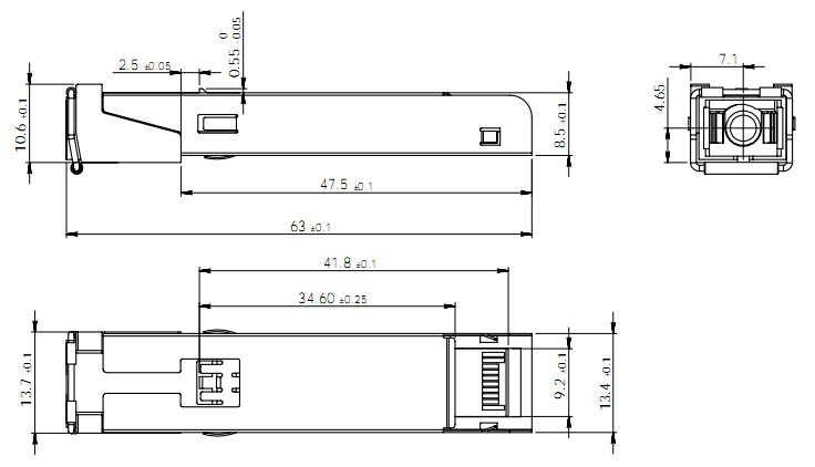
Package Diagram
Recommended Circuit
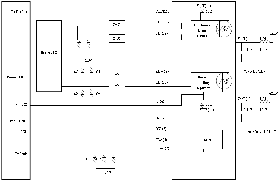
Note:
Tx:AC coupled internally.
R1=R2=150Ω.
Rx: LVPECL output, DC coupled internally.
Input stage in SerDes IC with internal bias to Vcc-1.3V
R3=R4=R5=R6=N.C
Input stage in SerDes IC without internal bias to Vcc-1.3V
R3=R4=130Ω, R5=R6=82Ω.
Timing Parameter Definition
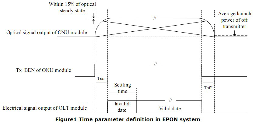
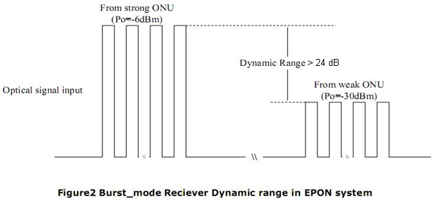
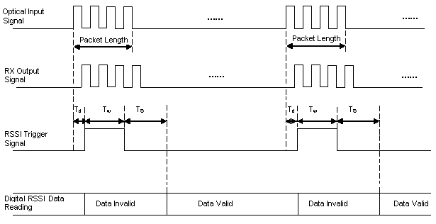
Timing Of Digital RSSI
|
PARAMETER |
SYMBOL |
MIN |
TYP |
MAX |
UNITS |
|
Packet Length |
- |
600 |
- |
- |
ns |
|
Trigger delay |
Td |
100 |
- |
- |
ns |
|
RSSI Trigger and Sample Time |
Tw |
500 |
- |
- |
ns |
|
Internal delay |
Ts |
500 |
- |
- |
us |
Change History
|
Version |
Change Description |
Issued By |
Checked By |
Appoved By |
Release Date |
|
A |
Initial release |
2016-01-18 |
| REV: | A |
| DATE: | August 30,2012 |
| Write by: | HDV phoelectron technology LTD |
| Contact: | Room703,Nanshan district science college town, Shenzhen, China |
| WEB: | Http://www.hdv-tech.com |