|
Part No. |
Wavelength |
Connector |
Temp. |
TX Power (dBm) |
RX Sens (Max.) (dBm) |
Distance |
|
SFP3524-F11LC-20 |
T 1310FP/R 1550 |
LC |
-20 to 70 |
-9 to-3 |
-21 |
20km |
|
SFP5324-D11LC-20 |
T 1550DFB/R 1310 |
LC |
-20 to 70 |
-15 to-3 |
-21 |
|
|
SFP5324-D11LC-40 |
T 1550DFB/R 1310 |
LC |
-20 to 70 |
-9 to-3 |
-24 |
40km |
|
SFP3524-D11LC-40 |
T 1310DFB/R 1550 |
LC |
-20 to 70 |
-5to-0 |
-24 |
|
|
SFP5424-D11LC-80 |
T 1550DFB/R 1490 |
LC |
-20 to 70 |
-3 to2 |
-26 |
80km |
|
SFP4524-D11LC-80 |
T 1490DFB/R 1550 |
LC |
-20 to 70 |
-3 to2 |
-26 |
|
Sign |
Mean |
Description |
|||||
|
SFP |
Module type |
SFP=Single fiber SFP transceiver |
|||||
|
35 |
Center wave |
35=1310tx/1550rx |
53=1550tx/1310rx |
45=1490tx/1550rx |
54=1550tx/1490rx |
||
|
24 |
Transmitter Rate |
03=155M |
03=622M |
24=1.25G |
48=2.5G |
60=3.125G |
|
|
F |
Laser type |
F=FP |
D=DFB |
C=CWDM |
V=VCSEL |
||
|
1 |
Operating T |
1=0~+70℃ |
2=-40~+85℃ |
||||
|
2 |
DDMI |
1=NO DDM |
2=DDMI |
||||
|
LC |
Connector |
SC=SC |
LC=LC |
||||
|
20 |
Distance |
022=220M |
055=550M |
5=5KM |
10=10KM |
||
|
20=20KM |
40=40KM |
80=80KM |
100=100KM |
||||
|
Parameter |
Symbol |
Min |
Max |
Unit |
|
|
Storage Temperature |
TS |
-40 |
+85 |
℃ |
|
|
Operating Temperature |
TOP |
Commercial level |
-20 |
+70 |
℃ |
|
industrial level |
-40 |
85 |
|||
|
Supply Voltage |
VCC |
-0.5 |
+4.5 |
V |
|
|
Voltage on Any Pin |
VIN |
0 |
VCC |
V |
|
|
Soldering Temperature ,Time |
- |
260℃, 10 S |
℃,S |
||
|
Parameter |
Symbol |
Min. |
Typ |
Max. |
Unit |
|
|
Ambient Temperature |
TAMB |
Commercial level |
0 |
- |
70 |
℃ |
|
industrial level |
-40 |
85 |
||||
|
Power Supply Voltage |
V CC-VEE |
3 |
3.3 |
3.6 |
V |
|
|
Parameter |
Symbol |
Min. |
Typ |
Max. |
Unit |
|||||
|
Center Wavelength |
lc |
1520 |
1550 |
1580 |
nm |
|||||
|
1280 |
1310 |
1340 |
||||||||
|
1470 |
1490 |
1510 |
||||||||
|
Spectral width |
△l |
FP@RMS |
- |
2 |
4 |
nm |
||||
|
DFB@-20dB FWHM |
- |
- |
1 |
|||||||
|
Output Power |
0~20km |
1.25G |
1310 FP |
Po |
-9 |
- |
-3 |
dBm |
||
|
14/15 DFB |
-15 |
-3 |
||||||||
|
40km |
1.25G |
14/15 DFB |
-9 |
- |
-3 |
|||||
|
1310 DFB |
-5 |
-0 |
||||||||
|
60km |
1.25G |
14/15 DFB |
-5 |
0 |
||||||
|
80km |
1.25G |
14/15 DFB |
-3 |
2 |
||||||
|
100~120km |
1.25G |
14/150 DFB |
0 |
3 |
||||||
|
Extinction Ratio |
ER |
9 |
- |
dB |
||||||
|
Supply Current |
ICCT |
- |
150 |
mA |
||||||
|
Input Differential Impedance |
Rin |
100 |
Ω |
|||||||
|
Data Input Swing Differential |
Vin |
300 |
1200 |
mV |
||||||
|
Optical Modulation Amplitude |
OMA |
174 |
μW |
|||||||
|
Transmit Disable Voltage |
VD |
2.0 |
Vcc |
V |
||||||
|
Transmit Enable Voltage |
VEN |
0 |
0.8 |
V |
||||||
|
Transmit Disable Assert Time |
10 |
us |
||||||||
|
Optical Rise/Fall Time |
1.25G |
Tr/ Tf (20-80%) |
150 |
260 |
ps |
|||||
|
Deterministic Jitter Contribution |
TX ΔDJ |
20 |
56.5 |
ps |
||||||
|
Total Jitter Contribution |
TX ΔTJ |
50 |
119 |
ps |
||||||
|
Parameter |
Symbol |
Min. |
Typ |
Max. |
Unit |
|||
|
Wavelength Range |
lc |
1520 |
1550 |
1580 |
nm |
|||
|
1280 |
1310 |
1340 |
||||||
|
1470 |
1490 |
1510 |
||||||
|
Sensitivity |
20km |
1.25G |
Pin |
PMIN |
- |
- |
-21 |
dBm |
|
40/60km |
1.25G |
Pin |
- |
- |
-24 |
|||
|
80km |
1.25G |
Pin |
- |
- |
-26 |
|||
|
100km |
1.25G |
APD |
-30 |
|||||
|
120km |
1.25G |
APD |
-32 |
|||||
|
MAX. Input Power (Saturation) |
PMAX |
-3 |
- |
- |
||||
|
Signal Detect Assert |
PA |
- |
- |
-24 |
||||
|
Signal Detect De-assert |
PD |
-45 |
- |
- |
||||
|
Signal Detect Hysteresis |
PHYS |
1 |
- |
4 |
||||
|
Supply Current |
ICCR |
- |
- |
150 |
mA |
|||
|
Data Output Swing Differential |
Vout |
400 |
- |
1000 |
mV |
|||
|
Signal Detect Voltage – High |
VSDHC |
2.0 |
- |
VCC |
V |
|||
|
Signal Detect Voltage – Low |
VSDL |
0 |
- |
0.8 |
||||
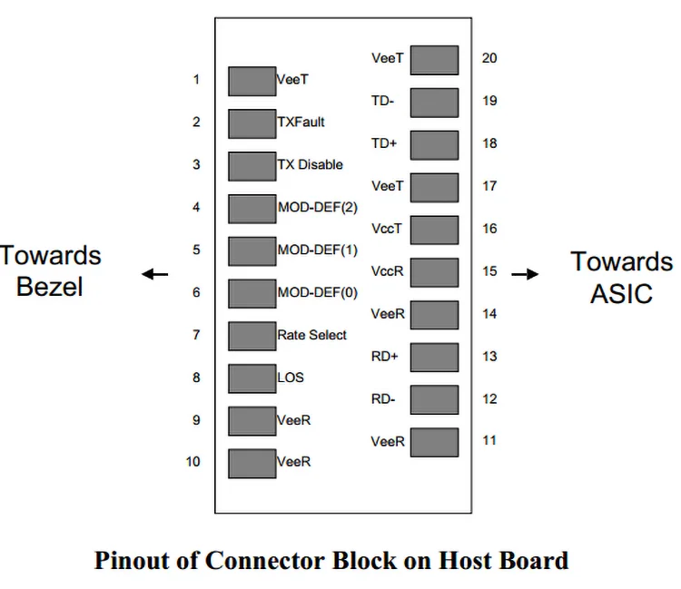
|
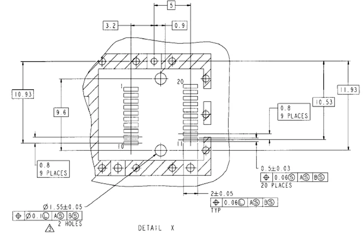
Pin |
Descriptions |
Pin |
Descriptions |
|
1 |
VEET |
Transmitter Ground (Common with Receiver Ground) |
1 |
|
2 |
TFAULT |
Transmitter Fault. |
2 |
|
3 |
TDIS |
Transmitter Disable. Laser output disabled on high or open. |
3 |
|
4 |
MOD_DEF(2) |
Module Definition 2. Data line for Serial ID. |
4 |
|
5 |
MOD_DEF(1) |
Module Definition 1. Clock line for Serial ID. |
4 |
|
6 |
MOD_DEF(0) |
Module Definition 0. Grounded within the module. |
4 |
|
7 |
Rate Select |
No connection required |
|
|
8 |
LOS |
Loss of Signal indication. Logic 0 indicates normal operation. |
5 |
|
9 |
VEER |
Receiver Ground (Common with Transmitter Ground) |
1 |
|
10 |
VEER |
Receiver Ground (Common with Transmitter Ground) |
1 |
|
11 |
VEER |
Receiver Ground (Common with Transmitter Ground) |
1 |
|
12 |
RD- |
Receiver Inverted DATA out. AC Coupled |
|
|
13 |
RD+ |
Receiver Non-inverted DATA out. AC Coupled |
|
|
14 |
VEER |
Receiver Ground (Common with Transmitter Ground) |
1 |
|
15 |
VCCR |
Receiver Power Supply |
|
|
16 |
VCCT |
Transmitter Power Supply |
|
|
17 |
VEET |
Transmitter Ground (Common with Receiver Ground) |
1 |
|
18 |
TD+ |
Transmitter Non-Inverted DATA in. AC Coupled. |
|
|
19 |
TD- |
Transmitter Inverted DATA in. AC Coupled. |
|
|
20 |
VEET |
Transmitter Ground (Common with Receiver Ground) |
1 |